
Latest News

Let our news appear at the top of your Google search results!
DI170SIC850D7 | Kelvin-Source Connectivity for Demanding Power Applications
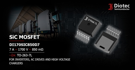
Designed for High-Voltage Power Conversion
Diotec Semiconductor has expanded its Silicon Carbide (SiC) MOSFET portfolio with the introduction of the DI170SIC850D7, a 1700 V device designed to address the growing demands of high-voltage power conversion applications. Featuring a maximum on-state resistance (RDS(on)) of 850 mΩ, the new MOSFET combines high-voltage capability with fast switching performance in a compact TO-263-7L package, also commonly referred to as D2PAK -7L.
A key feature of the package is its dedicated Kelvin-Source connection, which helps reduce the influence of parasitic inductance in the switching path. This enables faster and more controlled switching while contributing to lower switching losses and improved overall converter efficiency, while maintaining a compact footprint suitable for space-constrained PCB layouts.
The increasing use of higher DC input voltages in industrial equipment and renewable energy systems presents significant challenges for power-supply designers. In particular, efficiently converting high DC-link voltages into lower auxiliary supply rails requires switching devices that can withstand substantial voltage stress while maintaining high efficiency and a sufficient safety margin.
The DI170SIC850D7 has been developed with these requirements in mind. Its 1700 V drain-source breakdown voltage provides a substantial voltage margin for systems operating in the approximately 800 to 1000 VDC range, helping designers accommodate transient and parasitic voltage spikes that can occur during switching.
This makes the device particularly well suited to the implementation of compact and efficient flyback converters. Flyback topology remains a popular choice for isolated auxiliary power supplies due to its inherent simplicity, relatively low component count and integrated galvanic isolation.
Traditional silicon MOSFETs can face limitations in such applications, particularly when exposed to high voltage stress and high switching frequencies. The high-voltage capability and inherent characteristics of SiC technology allow the DI170SIC850D7 to operate efficiently under these demanding conditions.
SiC Technology for Efficient High-Frequency Switching
Silicon Carbide offers several advantages over conventional silicon power semiconductor technology. The material's low switching losses, high-temperature capability and strong avalanche ruggedness make SiC MOSFETs particularly attractive for high-frequency power-conversion applications.
In the DI170SIC850D7, these characteristics are combined with low capacitance, low gate charge and low total switching energy, supporting fast switching transitions while helping to minimize power losses.
The device also incorporates advanced planar technology and offers a low on-state resistance relative to its voltage rating. Together, these features help provide a balance between conduction losses, switching performance and thermal requirements.
These characteristics make the DI170SIC850D7 a suitable option for the next generation of high-voltage auxiliary power supplies, particularly where efficiency, isolation, switching speed and PCB space are important design considerations.
A High-Voltage Solution for Next-Generation Power Supplies
With its 1700 V voltage rating, 850 mΩ maximum RDS(on), fast-switching characteristics and Kelvin-Source contact, the DI170SIC850D7 provides designers with a compact SiC MOSFET solution for demanding high-voltage conversion applications.
The combination of SiC intrinsic material properties and the seven-lead D2PAK package enables efficient, high-frequency operation while helping designers manage voltage transients, switching losses and thermal constraints. As industrial, telecom and renewable-energy systems continue to move toward higher DC-link voltages, devices such as the DI170SIC850D7 can play an important role in developing compact and reliable auxiliary power supplies.
Features
- High reverse breakdown voltage VRRM
- Advanced Planar technology
- Low on-state resistance RDS(ON)
- Fast switching time with low capacitance
- Low Gate charge
- Low total switching energy
Applications
- Telecom power supplies
- Switched-mode power supply (SMPS)
- DC/DC converters
- Industrial machinery
Specifications
- 1700 V drain-source voltage (VDSS)
- Maximum 850 mΩ on-state resistance (RDS(on))
- 100 µA drain-source leakage current (IDSS)
- From to -10 V to 25 V continuous gate-source-voltage (VGSS)
- Recommended turn-on Gate voltage VGS(on)of 20 V
- Recommended turn-off Gate voltage VGS(off)of -5 V
- 62 W power dissipation (Ptot)
- Up to 9 A peak drain current (IDM)
- 1.8 K/W typical thermal resistance (RthC)
- -55°C to +175°C operating junction temperature range (Tj)
- TO-263-7L/ D2PAK with 7 leads
- Product families
- SiC MOSFETs en > productlist > SIC-FET